Engineered by experts. Verified by the data.
BPcore Silicon is an Indian semiconductor company based in Mumbai, Maharashtra. Our product, NeuraEdge v1.0, is a 256-MAC sparsity-aware NPU IP with a 7-stage ONNX compiler, full-layout physical signoff, and complete unencrypted RTL source delivery.
Why this. Why now.
The Push for True Independence
India is scaling domestic semiconductor capacity at a national level — fabrication facilities, design houses, and EDA infrastructure. But the critical IP blocks that define SoC capability remain controlled by foreign vendors. When Indian defence organisations and fabless companies license core accelerators from overseas, the supply chain carries structural geopolitical risk that no amount of domestic assembly can eliminate.
The Structural Liability of Licensed IP
The conventional IP licensing model extracts value from your success. A 3% royalty on a ₹400 ASP product at 1 million units is ₹12 Cr returned to a foreign IP holder — annually. That is not a vendor relationship. That is a structural financial liability embedded in your cost of goods sold.
A Better Way for Indian Business
BPcore Silicon operates on a single principle: one-time acquisition, zero recurring cost. The RTL, the compiler, the signoff data — all transferred in full. The IP becomes a capital asset on your balance sheet, not an operating expense. For Indian companies building at scale, this is the difference between renting capability and owning it.
The Engineering Truth Behind BPcore
If you cannot inspect it, you cannot trust it. Most tech companies hide their designs inside locked, encrypted "black boxes." We do the exact opposite.
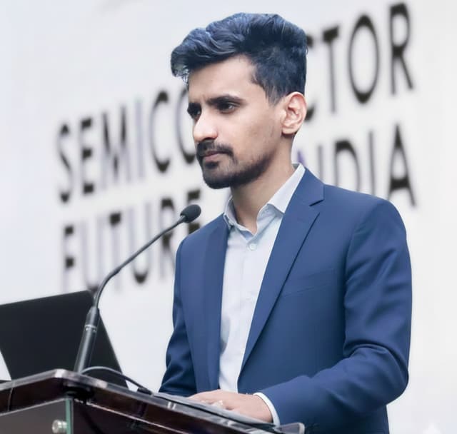
— Bandhan Patil, Founder & Chief Architect
The foundational vision of BPcore Silicon was shaped by our Founder and Chief Architect, Bandhan Patil. With a career built on years of hands-on industrial manufacturing experience combined with deep semiconductor design, Bandhan started the company to solve a glaring problem: the total lack of transparency in standard chip licensing.
Manufacturing teaches one absolute rule: if you cannot look inside a component, you cannot trust it. An encrypted foreign design is a black box. A fully readable, 91-file source tree is not.
Under Bandhan's architectural leadership, NeuraEdge was engineered to be exactly what the specification says it is. No estimates presented as measurements. No aspirational slides dressed as final data. Every number on this website traces directly back to a real engineering file or machine test output. That is not a marketing position; it is our minimum team standard for engineering honesty.
The goal is simple: give Indian semiconductor teams the absolute technological autonomy they deserve. One good AI chip design, fully owned, should be the launchpad for Indian hardware — not a recurring financial obstacle.
CORE VALUES & ENGINEERING PRINCIPLES
Four unshakeable principles.
Traditional technology vendors thrive on secrecy, complex contracts, and keeping their customers dependent. Our engineering and business teams operate on four simple principles that do the exact opposite.
Zero Black Boxes
Complete Ownership
Most tech companies sell you a locked design. You can use it, but you aren't allowed to see inside it or change it. We do the exact opposite. We hand over the complete, unlocked blueprint. If you buy it, you should own it — completely.
Total Source Transparency
Absolute Trust
By giving our customers fully readable source code, we remove the guesswork. Your teams can look at every single line of code to verify exactly how it works, how secure it is, and how it handles data.
Traceable Claims
No Marketing Fluff
The tech world is full of exaggerated promises. Every single speed, power, or cost-saving benchmark we show isn't an estimate — it is a proven fact traceable to tool outputs. If we can't prove it in the data, we don't say it.
India-First Design
Technological Sovereignty
For decades, India has provided the brainpower to design chips for global corporations, only to buy back the finished tech at a premium. We build specifically to empower the domestic ecosystem, keeping the ownership and financial upside inside the country.
PROCESS & METHODOLOGY
How we build.
Engineering truth requires an uncompromising process. We don't just write code; we subject our blueprints to some of the most punishing verification protocols in the industry.
NVLP Verification Protocol
Zero Blind Spots
A chip design is only as good as the tests it survives. Our team uses the NVLP (NeuraEdge Verification Logic Protocol) — a rigorous, custom-built testing framework that simulates thousands of real-world scenarios. We stress-test the architecture against edge cases, extreme workloads, and data bottlenecks to ensure there are zero hidden bugs. If it doesn't pass the protocol, it doesn't ship.
Open-Source Toolchains
Auditable Results
All initial signoff was performed using open-source EDA tools — Yosys, OpenSTA, OpenROAD, Magic, and Icarus Verilog — ensuring any buyer can reproduce our benchmarks without proprietary license dependencies. The RTL is lint-clean and structured for immediate ingestion into Synopsys DC, Cadence Genus, and PrimeTime flows. Commercial-tool signoff is a v2.0 commitment.
Rigorous Signoff Methodology
The Final Stamp of Proof
"Signoff" is the final stage before a blueprint is sent to a factory to be physically manufactured. A mistake here costs millions of dollars. Our signoff methodology simulates the actual, physical reality of the silicon — down to the microscopic timing of electrical signals and the exact physical space the chip will take up. We do not use estimates or "best-case" scenarios. When we hand over our design, it has already been mathematically proven to survive the physics of manufacturing.
OUR TEAM
Cross-functional expertise.
While the architectural vision began with Bandhan, delivering a production-ready chip design requires a highly synchronized, multi-disciplinary effort. BPcore Silicon operates with a specialized engineering team covering VLSI architecture, physical design verification, compiler development, and commercial operations. Post-NDA engagements include direct access to the architecture and verification engineers who built and signed off the NeuraEdge IP.
VLSI Design & Physical Validation
Our core engineering group executes the full layout, optimization, and rigorous testing of our chip blueprints. They make sure the code is completely clean, stable, and ready to be manufactured without risk of failure.
Commercial Strategy & Partnerships
Our business development unit handles ecosystem integration. They work directly with Indian fabless companies to structure clean, frictionless asset transfers, wiping out the traditional legal hassles of the IP industry.
Corporate Operations & Governance
Our operations team anchors the company's institutional stability and security compliance, ensuring we are a rock-solid partner capable of meeting the strict data and security requirements of national defense contractors.
MISSION
What we build
Production-grade AI chip blueprints that Indian semiconductor teams can acquire, own, and build upon — without royalties, without encrypted black boxes, and without foreign exposure.
How we verify it
Every claim traces to a source file. Every benchmark notes its exact test environment. Every disclosure is honest, including the features still in active development.
Why it matters
India is building chip design capacity at a national scale, and the foundation must be indigenously owned. What we architect today, the domestic industry will harvest for the next two decades.
Ready to own your architecture?
Schedule a direct technical consultation with our engineering leadership. No pitch decks. No sales reps. Just a 30-minute architect-to-architect review of your requirements.